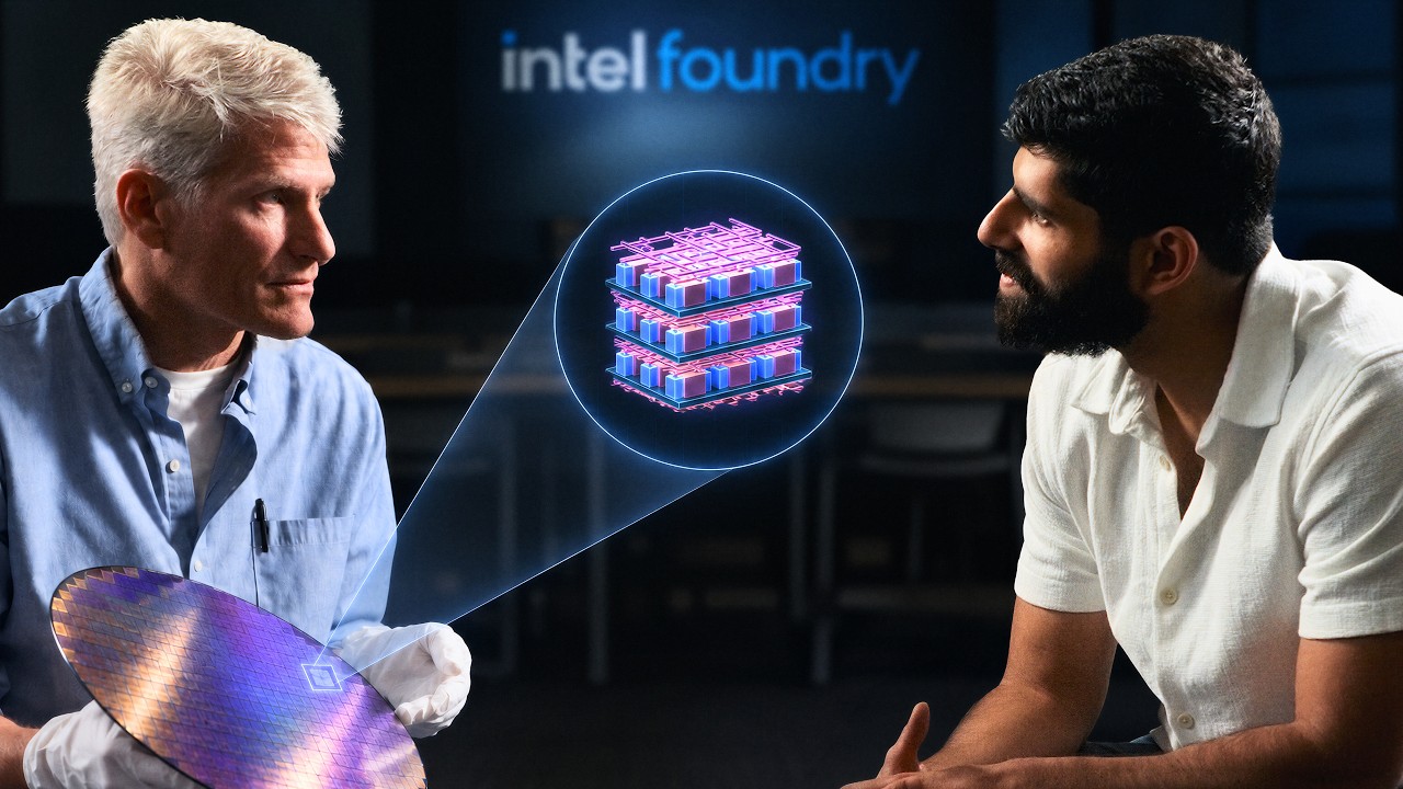
This episode explores Intel’s semiconductor manufacturing roadmap through interviews with its process development, packaging, and leadership teams, revealing how the company is racing to meet explosive AI-driven demand while transitioning to a foundry model, overcoming past delays, and pushing transistor architecture toward gate-all-around, backside power, CFET stacking, and hybrid bonding — all constrained by a brittle global supply chain for EUV tools.
14A process development and yield improvement
14A has been in development for over three years and is now in the finalization phase, locking down tool sets and fine-tuning roughly 2,000 factory steps for high-volume, repeatable manufacturing.
Yield improvement runs on a continuous loop: inline metrology tools flag defects on wafers in real time, while end-of-line electrical test and sort identify failing die; engineers cross-section defects (using TEM) to pinpoint the offending process module, then target the inline metrology signals from that module.
Intel uses maturity metrics and phase gates — yield, defect, and performance criteria — to decide whether a new feature graduates from pathfinding into development; anything that misses a gate gets deferred to the next node to protect schedule predictability.
A tiered “hot box” system prioritizes critical experimental lots: HotBox 1 races through the fab with priority at every tool, but disrupts overall factory efficiency, so it is reserved for the highest-impact yield limiters such as epitaxial nodules that short source/drain regions.
Lessons from 10 nm and EUV adoption
10 nm (originally targeted for 2016, shipped 2018) pursued aggressive “hyperscaling” without EUV, forcing complex multi-patterning workarounds that burdened process engineers and delayed the node; the technology ultimately achieved world-class yield, performance, and cost, but the schedule slip was costly.
The core lesson: limit the number of simultaneous innovations per node to maintain a predictable cadence; EUV was the key technology that should have been saved for a later node instead of being worked around.
TSMC adopted EUV in volume manufacturing in 2019 (5 nm in 2020), giving it roughly four more years of EUV experience before Intel’s first EUV products arrived in 2023.
Transistors evolved from planar (gate on top only) to FinFET (gate wraps three sides of a vertical fin, volume production at Intel in 2011) to gate-all-around (gate wraps all four sides of horizontal nanosheet ribbons).
Gate-all-around was demonstrated in 1988 but did not reach production until Samsung in 2022; the decade-plus gap reflects the need to solve integration challenges: placeholder sacrificial layers that survive 1,000 °C anneals, selective etch to release ribbons, conformal high-k/metal-gate fill, and new materials/tools from vendors.
R&D shifted from pure Dennard scaling (shrink everything) to a “golden age of innovation” — strained silicon, high-k/metal gate, FinFET, gate-all-around, backside power — expanding the material set ~10× and using atomic-layer deposition for atomic-scale control.
High-NA EUV and backside power
High-NA EUV (NA 0.55 vs. 0.33) prints features ~1.7× smaller in a single pass, reducing multi-patterning passes on $200 M+ tools; Intel adopts it for 14A, TSMC defers, citing economics.
The difference stems from backside power: Intel moves thick power lines to the wafer backside, relaxing front-side pitch so High-NA can print critical layers in one pass; TSMC keeps power on the front side, requiring tighter pitches that still need double-patterning even with High-NA.
Backside power is offered as a PDK option for 14A, with customer-by-customer discussion on the value/complexity trade-off.
Foundry transition and PDK development
Intel’s IDM history meant informal data sharing with internal product teams; becoming a merchant foundry required building a formal Process Design Kit (PDK) with maturity levels (0.5 → 0.9 → 1.0).
18A launched without a mature PDK, prompting customer feedback on quality and completeness; Intel has since incorporated that feedback, and 14A will have a high-quality PDK from day one.
Serving multiple customers gives foundries more wafers for learning, more revenue to reinvest, and stronger deadline discipline — advantages TSMC enjoyed for decades.
Future materials and architectures: ruthenium, CFET, 2D materials
Ruthenium is being explored to replace copper for the tightest interconnect pitches (~20 nm): copper needs a resistive liner/barrier that consumes cross-section; ruthenium can be etched directly, eliminating the liner and winning on effective resistivity at scaled dimensions.
CFET (complementary FET) stacks n-type and p-type gate-all-around transistors vertically, potentially doubling density; the challenge is vertical interconnects between stacked devices — high-aspect-ratio etch and void-free fill of deep, narrow trenches.
Research uses short-loop test vehicles (diodes, capacitors, single-ribbon CFETs) to de-risk individual process modules before integrating full stacks; feature sizes in the lab are already at production scale, but thousands of steps must converge to beat the incumbent side-by-side architecture.
2D materials (transition-metal dichalcogenides, monolayer-thick) are deposited and characterized in the lab for conductivity, contactability, and gate modulation, but face adhesion and hermeticity issues during subsequent processing.
Chris Auth notes that 3D logic stacking (transistors → interconnect → more transistors) is the long-term trajectory, analogous to 3D NAND, but heat removal is the fundamental limiter for logic; system-level thermal simulation is in its infancy.
Advanced packaging and hybrid bonding
Hybrid bonding fuses copper interconnects of two chips directly (no solder bumps), enabling sub-10 µm pitch today and demonstrated reliability at 0.45 µm pitch — an order-of-magnitude density runway.
Two flows: wafer-to-wafer (dominant in CMOS image sensors, requires matched known-good-die maps) and die-to-wafer (singulated known-good die bonded to known-good wafer sites, higher yield for logic-to-logic).
Beyond AI, hybrid bonding reduces picojoules/bit for CPU–GPU links in client devices, lowering system power and heat.
Supply chain bottlenecks and capacity scaling
ASML produces <100 EUV tools/year with no plan to significantly increase by 2030; capacity is split among Intel, TSMC, Samsung, and memory makers (SK Hynix, etc.).
Every process node locks in specific tools from single suppliers; shortages extend across the equipment base, not just EUV.
Intel aims for ~80% tool fungibility from 18A to 14A to preserve ramp flexibility; even with infinite CapEx, leading-edge wafer output could at most ~2× from current levels because yields are already high and marginal gains are hard.
AI compute demand has been ~3×/year; silicon supply cannot match that without the entire supply chain (tools, sub-suppliers, power, water, consumables) scaling in lockstep.
Economics, CapEx, and catching up to TSMC
Foundry economics are dominated by fixed costs (~80% of cost structure); every extra percent of utilization and yield delivers disproportionate revenue, driving consolidation to three advanced-node foundries.
Intel disputes direct density comparisons (e.g., 14A vs. TSMC N2) but acknowledges being within a few percent on performance/power/area; competitive parity across the full portfolio (multiple transistor flavors, SRAM variants, analog/RF) and on-time, high-yield ramps matter more than single-metric benchmarks.
TSMC ~$50 B CapEx (2024) vs. Intel ~$20 B; the gap reflects TSMC’s pure-play foundry scale vs. Intel’s still largely internal demand, but Intel expects its CapEx to grow as external foundry revenue ramps.
Intel sold its DRAM business (1980s) and flash business (recently); in hindsight, flash sale timing was poor given today’s memory supply crunch, which Auth argues is tighter than the logic crunch.
Radical manufacturing ideas and long-term outlook
Fab construction cost doubles every 4–5 years; High-NA EUV scanner + support ~$400 M today; extrapolating leads to unsustainable economics, prompting questions about whether clean rooms, process flows, and transistor designs locked in decades ago are still optimal.
Auth suggests “clean-slate” rethinking: could relaxed contamination control work? Could chip design methodologies from 30 years ago be overhauled? Incumbents won’t risk such experiments, but new entrants might.
On a 20-year horizon (2045), Auth envisions exotic 3D structures with transistors, interconnect, and memory monolithically integrated, but visibility beyond ~4 years is low; progress comes from solving the next four-year horizon, then the next.